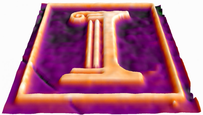
A three-dimensional image of an etched gallium-arsenide semiconductor, taken during etching with a new microscopy technique that monitors the etching process on the nanometer scale. The height difference between the orange and purple regions is approximately 250 nanometers.
CHAMPAIGN, Ill. University of Illinois researchers have a new low-cost method to carve delicate features onto semiconductor wafers using light - and watch as it happens. "You can use light to image the topography and you can use light to sculpture the topography," said electrical and computer engineering professor Gabriel Popescu. "It could change the future of semiconductor etching." Chip makers and semiconductor researchers need to very precisely control the dimensions of their devices. The dimensions of the components affect performance, speed, error rate and time to failure. Semiconductors are commonly shaped by etching with chemicals. Etching errors, such as residual layers, can affect the ability to further process and etch as well as hamper device performance.
TO READ THIS ARTICLE, CREATE YOUR ACCOUNT
And extend your reading, free of charge and with no commitment.