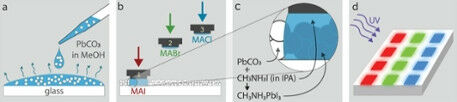
Schematic illustration showing the fabrication of a spatially patterned perovskite film. a) Drop casting PbCO3 particles dispersed in methanol onto a glass substrate results in a PbCO3 thin film that acts as the reactive canvas. b) Stamping MAX in IPA on the canvas results in, c) spatially-controlled conversion of the PbCO3 into a MAPbX3 perovskite. d) Upon UV irradiation, the converted areas emit light with a color that is controlled by adjusting the halide moiety of the perovskite. Image: AMOLF / Advanced Materials
Schematic illustration showing the fabrication of a spatially patterned perovskite film. a) Drop casting PbCO3 particles dispersed in methanol onto a glass substrate results in a PbCO3 thin film that acts as the reactive canvas. b) Stamping MAX in IPA on the canvas results in, c) spatially-controlled conversion of the PbCO3 into a MAPbX3 perovskite. d) Upon UV irradiation, the converted areas emit light with a color that is controlled by adjusting the halide moiety of the perovskite. Image: AMOLF / Advanced Materials Novel technique for spatially controlled deposition of semiconductors within one single layer 13 April 2021 Amsterdam researchers have developed a novel technique for spatially controlled patterning of semiconductors with tuneable optoelectronic properties. As a proof of principle, Lukas Helmbrecht and Wim Noorduin 'painted' a portrait of Marie Curie in a perovskite semiconductor layer. Both researchers work at the AMOLF research institute at Amsterdam Science Park.
TO READ THIS ARTICLE, CREATE YOUR ACCOUNT
And extend your reading, free of charge and with no commitment.