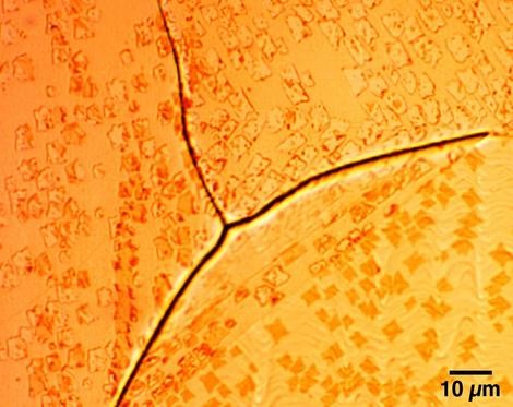
Optical micrograph showing graphene domains formed across grain boundaries.
A new way of growing graphene without the defects that weaken it and prevent electrons from flowing freely within it could open the way to large-scale manufacturing of graphene-based devices with applications in fields such as electronics, energy, and healthcare. A team led by Oxford University scientists has overcome a key problem of growing graphene - a one atom-thick layer of carbon - when using an established technique called chemical vapour deposition, that the tiny flakes of graphene form with random orientations, leaving defects or 'seams' between flakes that grow together. The discovery, reported in a paper to be published in ACS Nano , reveals how these graphene flakes, known as 'domains', can be lined up by manipulating the alignment of carbon atoms on a relatively cheap copper foil - the atomic structure of the copper surface acts as a 'guide' that controls the orientation of the carbon atoms growing on top of them. A combination of control of this copper guide and the pressure applied during growth makes it possible to control the thickness of these domains, the geometry of their edges and the grain boundaries where they meet - 'seams' that act as obstacles to the smooth progress of electrons necessary to create efficient graphene-based electrical and electronic devices. 'Current methods of growing flakes of graphene often suffer from graphene domains not lining up,' said Nicole Grobert of Oxford University's Department of Materials who led the work.
TO READ THIS ARTICLE, CREATE YOUR ACCOUNT
And extend your reading, free of charge and with no commitment.