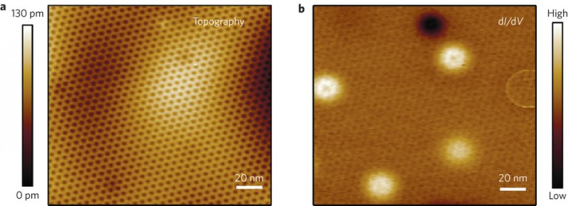
(a) STM topographic image of a clean graphene/BN area (b) dI/dV map acquired simultaneously with (a) exhibits new features including bright dots, a dark dot and a ring.
Berkeley Lab researchers characterize individual defects inside a bulk insulator using scanning tunneling microscopy. Nanoscale defects are enormously important in shaping the electrical, optical, and mechanical properties of a material. For example, a defect may donate charge or scatter electrons moving from one point to another. However, observing individual defects in bulk insulators, a ubiquitous and essential component to almost all devices, has remained elusive: it's far easier to image the detailed electrical structure of conductors than insulators. Now, Berkeley Lab researchers have demonstrated a new method that can be applied to study individual defects in a widely used bulk insulating material, hexagonal boron nitride (h-BN), by employing scanning tunneling microscopy (STM). "Normally, STM is used to study conductors and cannot be used to study bulk insulators, since electrical current does not typically flow through an insulator," explains Mike Crommie, physicist at Berkeley Lab's Materials Sciences Division and professor at UC Berkeley, in whose lab this work was conducted. His team overcame this obstacle by capping the h-BN with a single sheet of graphene.
TO READ THIS ARTICLE, CREATE YOUR ACCOUNT
And extend your reading, free of charge and with no commitment.