Nanoworld in 3D.
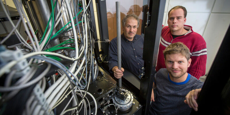
Gaining detailed knowledge about atomic structure and chemical composition is paramount for a deeper understanding of the properties of matter and their potential applications in technology. Electron microscopy thus represents a key tool for the comprehensive characterization of materials at highest spatial resolution in three dimensions. Atomic-scale defects already define electronic and optical properties of photonic and semiconducting materials, the location of dopant atoms determines the performance of silicon transistors and spintronic devices and the chemistry and orientation of surfaces and interfaces of metallic particles control their catalytic activity. Richard Feyman's challenge from 1959, to build a better microscope that allows for an identification of individual atoms in a chemical structure, could be tackled just recently with the realization of aberration-corrected electron microscopes. These sophisticatedly engineered systems consist of lens modules that can resolve object structures smaller than 100 picometer. The Center for Electron Microscopy Graz hosts one of these instruments ( ASTEM , Austrian Scanning Transmission Electron Microscope) since 2011 and operates it together with the Institute for Electron Microscopy FELMI at the TU Graz. With its configuration it is one of the most capable and enabling devices for material research world-wide.
TO READ THIS ARTICLE, CREATE YOUR ACCOUNT
And extend your reading, free of charge and with no commitment.