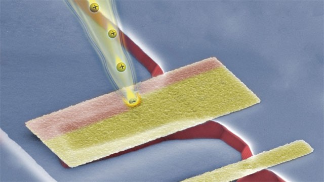
Schematic of the 3D printing process and an image of a manufactured microstructure
Reception and service at central level for international students after arrival at KTH. For Master's students For Exchange students At the KTH Symposium, the director of the U.S. National Science Foundation explains how scientific co-operation with Sweden benefits American research. AIMday Image is a forum for knowledge exchange between academic and industrial scientists in the field of image analysis Welcome to KTH on March 7! A drawing programme and a 3D printer: before long, that could be all it will take to produce the micro- and nanostructures required for the millions of devices and sensors of the future. With a new manufacturing technology, researchers at KTH Microsystem Technology hope to bring mass innovation capabilities to smaller companies and markets - just as affordable computers have dramatically extended information-sharing. Production of silicon micro- and nanosensors with today's technologies requires a full-scale clean-room laboratory costing millions of euros - facilities that few organisations can afford. What's more, integrated-circuit manufacturing technologies used in sensor production are highly standardised processes, optimised for extremely large production volumes of hundreds of millions of devices per year. These sensors, known as Micro Electromechanical Systems (MEMS), are engineered from thin slices of silicon, the same material used to manufacture integrated circuits and other micro-sized electronic devices.
TO READ THIS ARTICLE, CREATE YOUR ACCOUNT
And extend your reading, free of charge and with no commitment.