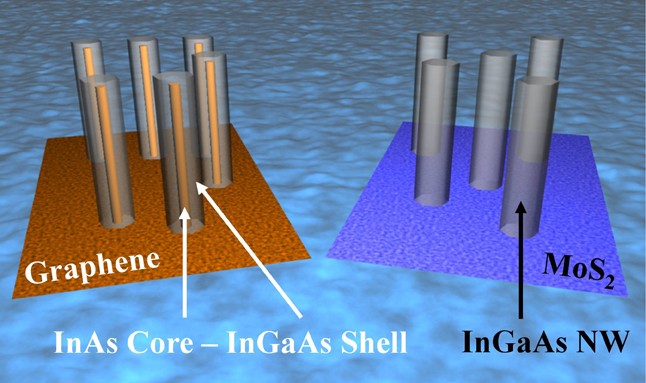
Schematic representation of phase segregated InGaAs/InAs nanowires grown on graphene and single phase InGaAs nanowires grown on a different substrate
CHAMPAIGN, Ill. When a team of University of Illinois engineers set out to grow nanowires of a compound semiconductor on top of a sheet of graphene, they did not expect to discover a new paradigm of epitaxy. The self-assembled wires have a core of one composition and an outer layer of another, a desired trait for many advanced electronics applications. Led by professor Xiuling Li, in collaboration with professors Eric Pop and Joseph Lyding, all professors of electrical and computer engineering, the team published its findings in the journal Nano Letters. Nanowires, tiny strings of semiconductor material, have great potential for applications in transistors, solar cells, lasers, sensors and more. "Nanowires are really the major building blocks of future nano-devices," said postdoctoral researcher Parsian Mohseni, first author of the study. "Nanowires are components that can be used, based on what material you grow them out of, for any functional electronics application." Li's group uses a method called van der Waals epitaxy to grow nanowires from the bottom up on a flat substrate of semiconductor materials, such as silicon.
TO READ THIS ARTICLE, CREATE YOUR ACCOUNT
And extend your reading, free of charge and with no commitment.