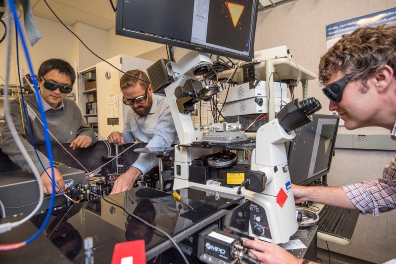
From left: Kaiyuan Yao, Nick Borys, and P. James Schuck, seen here at Berkeley Lab’s Molecular Foundry, measured a property in a 2-D material that could help realize new applications. (Credit: Marilyn Chung/Berkeley Lab)
Berkeley Lab-led team also provides most precise band gap measurement yet for hotly studied monolayer moly sulfide. Two-dimensional materials are a sort of a rookie phenom in the scientific community. They are atomically thin and can exhibit radically different electronic and light-based properties than their thicker, more conventional forms, so researchers are flocking to this fledgling field to find ways to tap these exotic traits. Applications for 2-D materials range from microchip components to superthin and flexible solar panels and display screens, among a growing list of possible uses. But because their fundamental structure is inherently tiny, they can be tricky to manufacture and measure, and to match with other materials. So while 2-D materials R&D is on the rise, there are still many unknowns about how to isolate, enhance, and manipulate their most desirable qualities. Now, a science team at the Department of Energy's Lawrence Berkeley National Laboratory (Berkeley Lab) has precisely measured some previously obscured properties of moly sulfide, a 2-D semiconducting material also known as molybdenum disulfide or MoS2.
TO READ THIS ARTICLE, CREATE YOUR ACCOUNT
And extend your reading, free of charge and with no commitment.