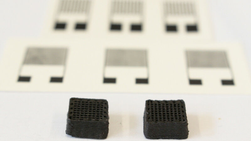
Novel material for printed circuits: Two test cuboids one centimeter wide from the 3D printer. The printed electronic sensors can be seen in the background. Image: Empa
Novel material for printed circuits: Two test cuboids one centimeter wide from the 3D printer. The printed electronic sensors can be seen in the background. Image: Empa - Intelligent packaging with sensors that monitor goods, such as vegetables, on long transport routes is a trend for the future. Yet printed and disposable electronics also cause problems: Metals in printing inks are expensive - and disposing of them in an environmentally sound manner is costly and exacerbates the problem of electronic waste. A new solution from researchers aims to remedy this. More precise, faster, cheaper: Researchers all over the world have been working for years on producing electrical circuits using additive processes such as robotic 3-printing (so-called robocasting) - with great success, but this is now becoming a problem. The metal particles that make such "inks" electrically conductive are exacerbating the problem of electronic waste.
TO READ THIS ARTICLE, CREATE YOUR ACCOUNT
And extend your reading, free of charge and with no commitment.