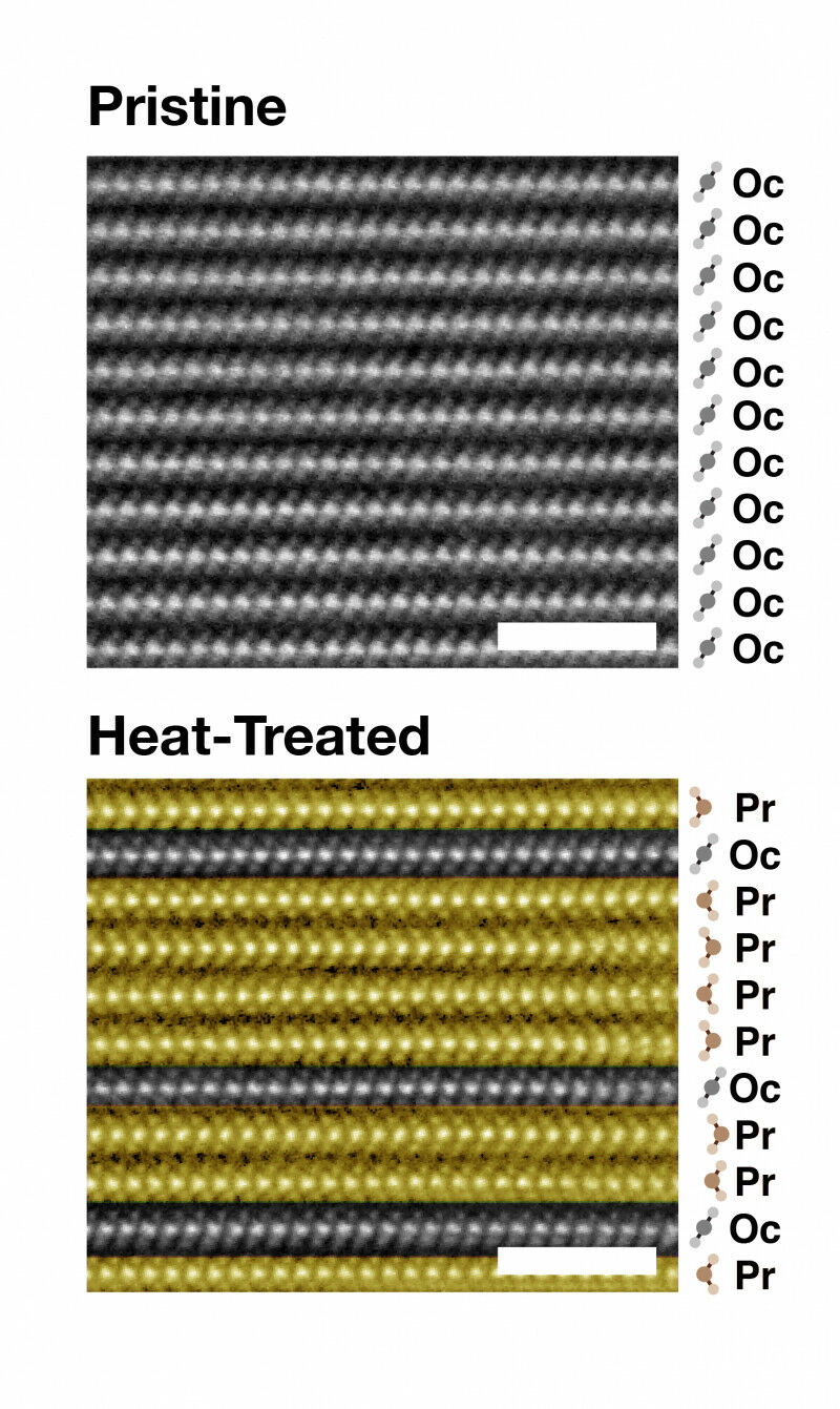
This electron microscopy image shows the atoms within individual two-dimensional layers of tantalum sulfide before and after the heat treating process. Before heat-treating, all layers are bonded with octahedral geometry. After heat-treating, most layers are bonded with prismatic geometry. The remaining octahedral layers exhibit ordered charged density waves and have switched from conductor to insulator. The white scale bar represents two nanometers. Image credit: Suk Hyun Sun
This electron microscopy image shows the atoms within individual two-dimensional layers of tantalum sulfide before and after the heat treating process. Before heat-treating, all layers are bonded with octahedral geometry. After heat-treating, most layers are bonded with prismatic geometry. The remaining octahedral layers exhibit ordered charged density waves and have switched from conductor to insulator. The white scale bar represents two nanometers. Image credit: Suk Hyun Sun A semiconducting material that performed a quantum "flip” from a conductor to an insulator above room temperature has been developed at the University of Michigan. It potentially brings the world closer to a new generation of quantum devices and ultra-efficient electronics.
TO READ THIS ARTICLE, CREATE YOUR ACCOUNT
And extend your reading, free of charge and with no commitment.