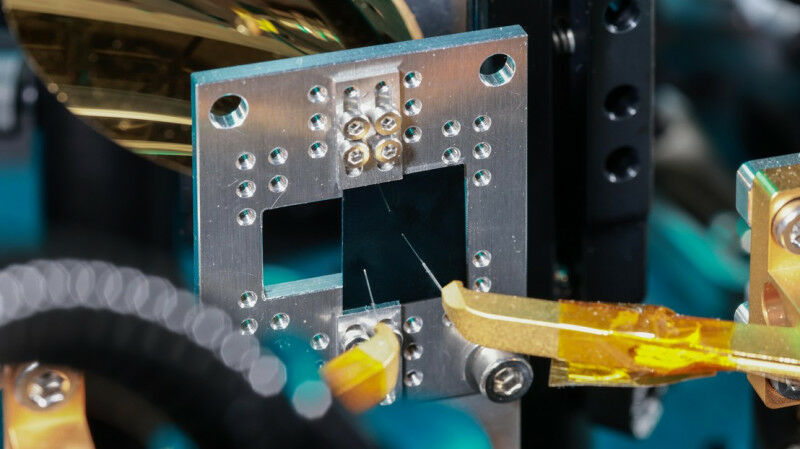
© Alain Herzog - Researchers have collaborated with those at Harvard and ETH Zurich on a new thin-film circuit that, when connected to a laser beam, produces finely tailorable terahertz-frequency waves. The device opens up a world of potential applications in optics and telecommunications. Researchers led by Cristina Benea-Chelmus in the Laboratory of Hybrid Photonics ( HYLAB ) in EPFL's School of Engineering have taken a big step toward successfully exploiting the so-called terahertz gap, which lies between about 300-30,000 gigahertz (0.3 to 30 THz) on the electromagnetic spectrum. This range is currently something of a technological dead zone, describing frequencies that are too fast for today's electronics and telecommunications devices, but too slow for optics and imaging applications. Now, thanks to an extremely thin chip with an integrated photonic circuit made of lithium niobate, the HYLAB researchers and colleagues at ETH Zurich and Harvard University have succeeded not just in producing terahertz waves, but in engineering a solution for custom-tailoring their frequency, wavelength, amplitude, and phase. Such precise control over terahertz radiation means that it can now potentially be harnessed for next-generation applications in both the electronic and optical realms. The results have recently been published in Nature Communications.
TO READ THIS ARTICLE, CREATE YOUR ACCOUNT
And extend your reading, free of charge and with no commitment.
Your Benefits
- Access to all content
- Receive newsmails for news and jobs
- Post ads