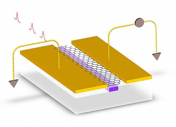
In a new graphene-on-silicon photodetector, electrodes (gold) are
deposited, slightly asymmetrically, on either side of a silicon waveguide
(purple). The asymmetry causes electrons kicked free by incoming light to
escape the layer of graphene (hexagons) as an electrical current.
Graphene - which consists of atom-thick sheets of carbon atoms arranged hexagonally - is the new wonder material: Flexible, lightweight and incredibly conductive electrically, it's also the strongest material known to man. In the latest , researchers at MIT, Columbia University and IBM's T. J. Watson Research Center describe a promising new application of graphene, in the photodetectors that would convert optical signals to electrical signals in integrated optoelectronic computer chips. Using light rather than electricity to move data both within and between computer chips could drastically reduce their power consumption and heat production, problems that loom ever larger as chips' computational capacity increases. Optoelectronic devices built from graphene could be much simpler in design than those made from other materials. If a method for efficiently depositing layers of graphene - a major area of research in materials science - can be found, it could ultimately lead to optoelectronic chips that are simpler and cheaper to manufacture. "Another advantage, besides the possibility of making device fabrication simpler, is that the high mobility and ultrahigh carrier-saturation velocity of electrons in graphene makes for very fast detectors and modulators," says Dirk Englund, the Jamieson Career Development Assistant Professor of Electrical Engineering and Computer Science at MIT, who led the new research.
TO READ THIS ARTICLE, CREATE YOUR ACCOUNT
And extend your reading, free of charge and with no commitment.