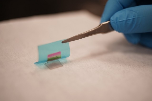
MIT researchers have devised a way to grow single crystal GaN thin film on a GaN substrate through two-dimensional materials. The GaN thin film is then exfoliated by a flexible substrate, showing the rainbow color that comes from thin film interference. This technology will pave the way to flexible electronics and the reuse of the wafers. Photo credits: Wei Kong and Kuan Qiao
Cost-effective method produces semiconducting films from materials that outperform silicon. The vast majority of computing devices today are made from silicon, the second most abundant element on Earth, after oxygen. Silicon can be found in various forms in rocks, clay, sand, and soil. And while it is not the best semiconducting material that exists on the planet, it is by far the most readily available. As such, silicon is the dominant material used in most electronic devices, including sensors, solar cells, and the integrated circuits within our computers and smartphones. Now MIT engineers have developed a technique to fabricate ultrathin semiconducting films made from a host of exotic materials other than silicon. To demonstrate their technique, the researchers fabricated flexible films made from gallium arsenide, gallium nitride, and lithium fluoride - materials that exhibit better performance than silicon but until now have been prohibitively expensive to produce in functional devices.
TO READ THIS ARTICLE, CREATE YOUR ACCOUNT
And extend your reading, free of charge and with no commitment.