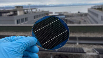
With a new technique, MIT researchers can peel and stack thin films of metal oxides - chemical compounds that can be designed to have unique magnetic and electronic properties. The films can be mixed and matched to create multi-functional, flexible electronic devices, such as solar-powered skins and electronic fabrics. Image: Felice Frankel
With a new technique, MIT researchers can peel and stack thin films of metal oxides - chemical compounds that can be designed to have unique magnetic and electronic properties. The films can be mixed and matched to create multi-functional, flexible electronic devices, such as solar-powered skins and electronic fabrics. Image: Felice Frankel Next-generation devices made with new "peel and stack" method may include electronic chips worn on the skin. Because computer chips are rigid, the electronic devices that they power, such as our smartphones, laptops, watches, and televisions, are similarly inflexible. Now a process developed by MIT engineers may be the key to manufacturing flexible electronics with multiple functionalities in a cost-effective way. The process is called "remote epitaxy" and involves growing thin films of semiconducting material on a large, thick wafer of the same material, which is covered in an intermediate layer of graphene. Once the researchers grow a semiconducting film, they can peel it away from the graphene-covered wafer and then reuse the wafer, which itself can be expensive depending on the type of material it's made from.
TO READ THIS ARTICLE, CREATE YOUR ACCOUNT
And extend your reading, free of charge and with no commitment.